


- 01 In-Situ Tensile Test
- 02 Simultaneous DIC
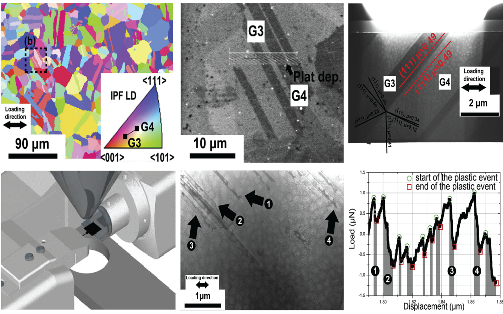
Simoultaneus Mechanical Testing with STEM and EBSD
In-situ tests of nickel-based superalloy oligocrystals in a scanning electron microscope revealed dislocation dynamics during tensile loading.
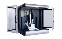
After selecting a proper location, in terms of microstructure and crystal orientation using SEM and EBSD, a specimen was extracted by focused-ion beam (FIB) machining, placed on a testing sample support (e.g. FemtoTool’s Nano-Tensile testing chip), and secured using Ion (or electron) beam induced deposition. FIB carving and thinning of the micro-tensile specimen down to electron transparency was then performed with low voltage to minimize FIB damage and enable STEM imaging.
Dislocation behavior near twin boundaries, precipitate shearing, and antiphase boundary-coupled shearing within slip bands was successfully revealed. These findings offer new insights into strain localization, plastic localization, and fatigue crack initiation near twin boundaries in superalloys.
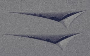
Micro-Shear of Silicon as Observed by Digital Image Correlation (DIC)
In this example, acquired in collaboration with the Laboratory for Nanometallurgy at ETH Zurich, [110]-oriented Silicon is sheared directly on its primary slip planes at 600 °C. Color strain maps are provided using digital image correlation (DIC) using the speckle patterns and in-situ imaging at temperature in the SEM. This enables direct measurement of the local strains within the shear zones.
More Applications
Nanoindentation
READ MORE ->
Read More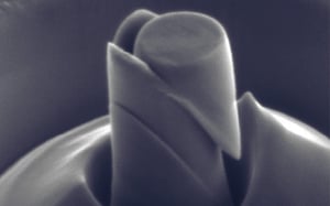
Micro-Pillar Compression
READ MORE ->
Read More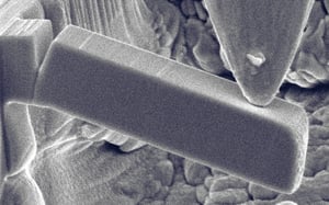
Micro-Cantilever Testing
READ MORE ->
Read More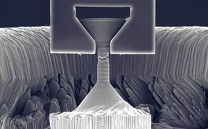
Micro-Tensile Testing
READ MORE ->
Read More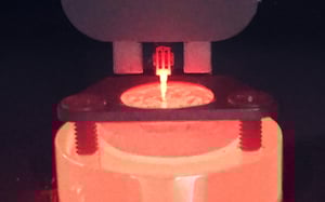
High-Temperature Testing
READ MORE ->
Read More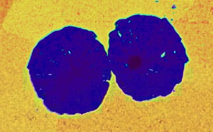
Mechanical Microscopy
READ MORE ->
Read More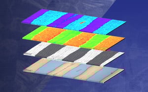
Correlative Mechanical Microscopy
READ MORE ->
Read More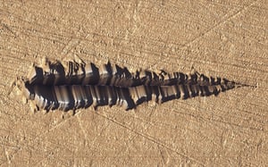
Scratch Testing
READ MORE ->
Read More