


- 01 Unmatched Dynamic Range
- 02 Highest Resolution
- 03 True Displacement Control
Micro-Electro-Mechanical System (MEMS)-based force sensors have an unmatched dynamic range of up to 100 kHz, thanks to their exceptionally small mobile mass and high stiffness. Moreover, the fine fabrication tolerances of MEMS achieve the lowest possible noise floor, reaching down to 500 pN.
|
up to 100 kHz |
down to 500 pN |
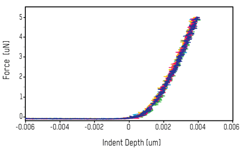
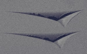
A key quality metric of a nanoindenter is its ability to accurately measure indentation depth. This is limited by the noise floor (resolution) of the displacement sensor. With an unmatched noise floor of <50 pm, the FT-I04 Femto-Indenter achieves excellent results even at the most shallow depths, as shown here with repeatable indentation curves to only 5 nm on quartz glass.
|
< 50 pm |
|
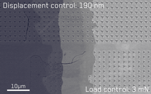
Displacement-controlled nanoindentation is essential for measuring and comparing mechanical properties at consistent indentation depths, ensuring the probing of equivalent material volumes.
|
Native displacement control |
Testing modes
Nanoindentation
Nanoindentation assesses the local mechanical behavior of a material by pressing a sharp tip into its surface and measuring the force needed to create an indent. This technique measures local mechanical properties (including hardness, elastic modulus, strain rate sensitivity, and others) directly from the material's response.
READ MORE ->
Read More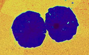
Mechanical Microscopy
Nanoindentation mapping, or mechanical microscopy, employs a nanoindenter in a microscope-like manner. It enables the mapping of mechanical properties of intricate microstructures in minutes, thanks to the integration of rapid indentation speeds and precise spatial resolution.
READ MORE ->
Read More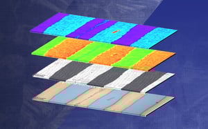
Correlative Mechanical Microscopy
Correlative mechanical microscopy merges nanoindentation with additional microscopy methods. This integration of various data layers enables precise phase identification by including elemental or crystallographic analysis in the mechanical measurement.
READ MORE ->
Read More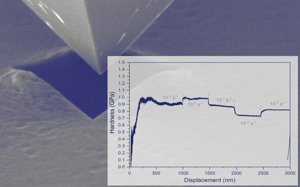
Strain-Rate Control
Time, like temperature, is a key parameter for materials deformation. Speed determines the active deformation mechanism. Strain-rate control during testing achieves the most consistent results and allows exploring the material's response from creep to impact, even within a single indent.
READ MORE ->
Read More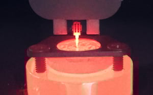
High-Temperature Testing
Temperature changes the mechanical behavior of materials. It is crucial for assessing operando mechanical properties, under conditions close to their target application. Using precision MEMS heating to achieve rapid temperature matching and thermal control, stable measurements can be performed even at high temperatures.
READ MORE ->
Read More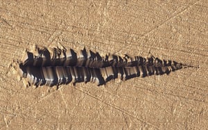
Scratch Testing
Scratch is a critical method for assessing materials’ adhesion, hardness, and resistance to wear - especially for coatings. It provides quantitative data on material durability and performance by scribing a hard tip across the surface and measuring the required force and the resulting topography.
READ MORE ->
Read More
Soft Materials Testing
Polymers, metamaterials, or bio-inspired materials are critical for modern technologies. Analysis of these soft materials requires systems capable of both large displacements and high force resolution.
READ MORE ->
Read More- 01 High-Temperature Module
- 02 Scratch Testing Module
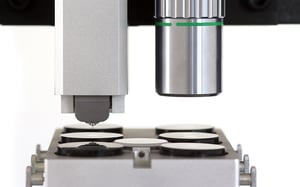
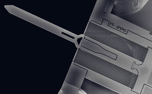
- 03 Microforce Sensing Probes
- 04 Two-Axis Microforce Probes
- 05 High-Temperature Probes
FT-HT04
High-Temperature Module
The high-temperature module enables mechanical testing, such as nanoindentation, at controlled temperatures up to 400°C in an inert gas atmosphere. In combination with our microforce sensing probes featuring tip heating, controlled isotherm testing is possible.
![]()
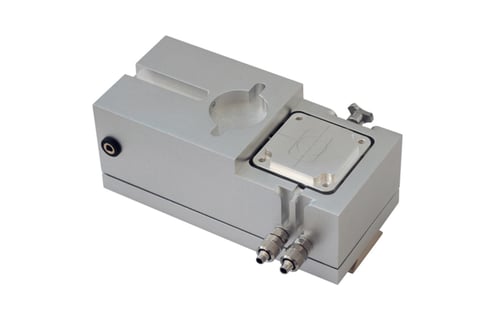
FT-ST04
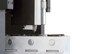
Scratch Testing Module
Combining an exchangeable sample stage with a piezoscanner and a FemtoTools 2-Axis Microforce Sensing Probe enables advanced techniques, such as nano-scratch and nano-wear testing, as well as SPM imaging, by facilitating the in-plane movement of the sample while simultaneously applying a normal force.
![]()
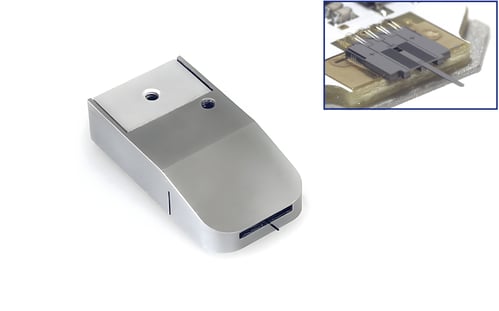
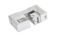
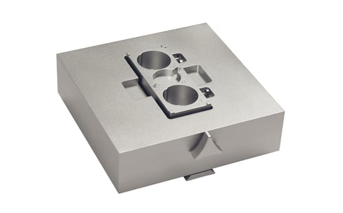
FT-S
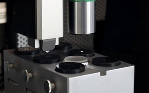
Microforce Sensing Probes
The FT-S Microforce Sensing Probes are sensors capable of measuring forces from sub-nanonewton to 2 newtons along the sensor’s probe axis. They are available with a wide variety of tip materials and geometries, including diamond Berkovich, cube corner, flat punch, wedge, conical, and more.
![]()
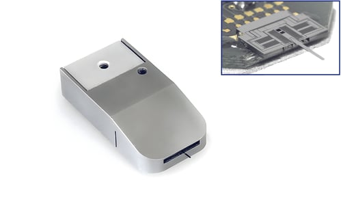
FT-S
Two-Axis Microforce Sensing Probes
The FT-S Two-Axis Microforce Sensing Probes are Micro-Electro Mechanical Systems (MEMS) based multi-axis microforce sensors capable of simultaneous measuring forces in the two in-plane directions. The primary application for these sensors is nano-scratch, nano-tribology and nano-wear testing.
![]()
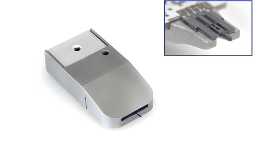
FT-S
High-Temperature Microforce Sensing Probes
The FT-S High-Temperature Microforce Sensing Probes are Micro-Electro Mechanical Systems (MEMS) based microforce sensors capable of measuring forces from 200mN to 2 µN. Furthermore, with the monolithically integrated tip heater, the temperature of the nanoindenter tip can be accurately matched to the temperature of the sample, enabling isothermal testing conditions.
![]()