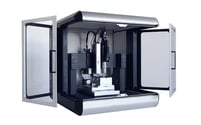
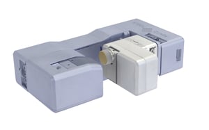
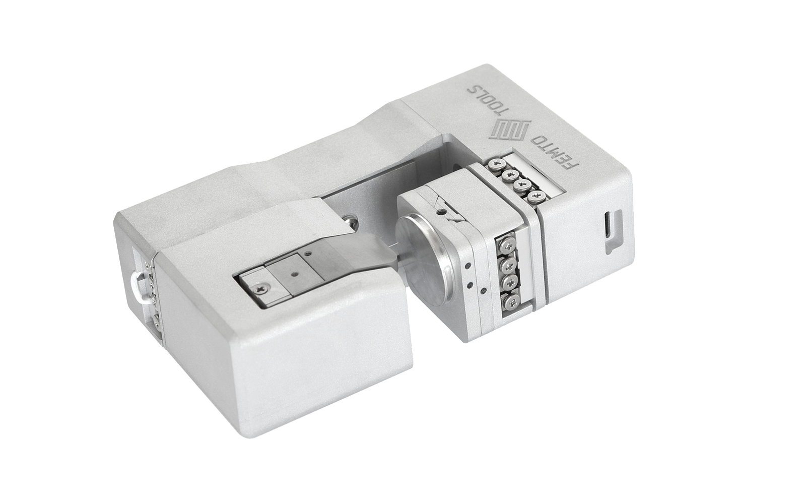
The FT-NMT04 can be upgraded with the FT-SEM-ST04 In-situ SEM Scratch Testing Module to allow for nano-scratch, nano-wear and nano-friction testing, as well as scanning probe microscopy (SPM). The diamond tip of a 2-Axis Microforce Sensing Probe is moved across the sample surface while applying a ramped or constant normal load at a given speed.
Scratch testing yields quantitative insights into various properties such as failure mechanisms at the nanoscale, thin film adhesion, friction coefficients, and abrasive or wear resistance of materials. Furthermore, high-resolution SPM imaging can be used for topographic imaging before and after scratch, wear, or nanoindentation testing. It provides direct visualization of pre-test surface roughness and post-test surface deformation or damage.